VIGILANT SENSOR

RF Voltage-Current Probe for Plasma Processing Applications (analog vi probe)
Users
Researchers
R&D engineers
Equipement maintenance engineers
Applications
Study of RF discharges
Development of processing tools
Troubleshooting of RF systems
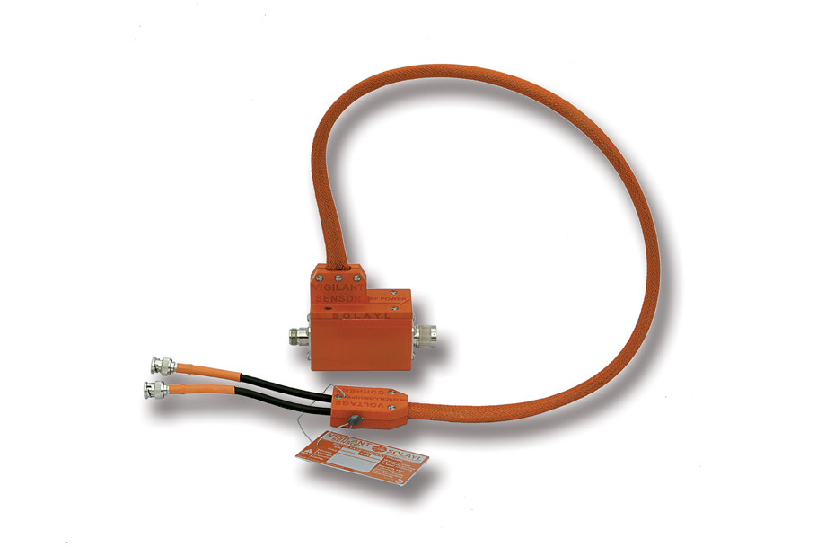


The Vigilant Sensor uses two innovative sensors to achieve accurate simultaneous measurements of both the voltage and current waveforms with a minimum perturbation. It delivers two analogs signals optimized for analysis by your test instrument (oscilloscope, spectrum analyzer). This analog vi probe can be used before or after the matching unit inside your plasma system.
We combine many proprietary innovations to offer what is probably the most advanced analog RF voltage-current probe commercially available today:
- Customizable high performance electrical sensors: wideband, robust, low-perturbative and compact voltage and current sensors developed through extensive experimental work and
electromagnetic modeling. The settings of these sensors are customized during calibration to maximize performance for your application (maximized sensitivity and power rating while minimizing the
perturbation).
- Automated highly accurate calibration process to ensure the best measurement accuracy and probe-to-probe repeatability. Our calibration process is NIST-traceable and uses the best electronic test instruments available today in a temperature and EMI controlled environment. Each probe is provided with its own certificate of calibration. The calibration is performed with the non-detachable signal cable.
Specifications
Frequency band
Max power
Calibration factors accuracy
Insertion Loss
Through-line
Signal cable
Size
1-150MHz
10kW
+/- 2% (typical)
<0.5% at the excitation frequency
50Ω coaxial line with customized input & output connectors
Pair of shielded 50Ω coaxial cables terminated with BNC connectors
90mm x 90mm x 45mm (without the signal cable)
Ordering information
In order to provide you with the best suitable probe for your application, please use the following model numbering:
VSN-FREQ-POWER-IN-OUT-LEN Example: VSN-13.56-1000-1F-1M-100
|
Code |
Details |
Values C: Custom (if not listed) |
| FREQ | Excitation frequency in MHz | 2, 3.39, 4, 6.78, 13.56, 27.12, 40.68, 60, 81.36 |
|
POWER |
Max generator power in Watt | 30, 60, 100, 300, 600, 1000, 3000, 6000, 10000 |
|
IN
OUT |
Input connector type and gender Output connector type and gender |
0: No connector (M5 threaded hole)
1F: N Female 1M: N Male 2F: HN Female 2M: HN Male 3F: 7/16 Female 3M: 7/16 Male 4F: LC Female 4M: LC Male |
|
LEN |
Length of the signal cable in cm | Between 30 and 300 (100 by default) |
Datasheet
Citations in peer-reviewed journals
2016
Experimental and simulation study of a capacitively coupled oxygen discharge driven by tailored voltage waveforms
Aranka Derzsi1, Trevor Lafleur2, Jean-Paul Booth2, Ihor Korolov1 and Zoltán Donkó1
1 Institute for Solid State Physics and Optics, Wigner Research Centre for Physics, Hungarian Academy of Sciences, 1121 Budapest, Konkoly Thege Miklós str. 29-33, Hungary
2 Laboratoire de Physique des Plasmas, Ecole Polytechnique-CNRS-Univ Paris-Sud-UPMC, 91128 Palaiseau, France
Abstract
We report experimental and particle-based kinetic simulation studies of low-pressure capacitively coupled oxygen plasmas driven by tailored voltage waveforms that consist of up to four harmonics of base frequency 13.56 MHz. Experimentally determined values of DC self-bias and electrical power deposition, as well as flux density and flux-energy distribution of the positive ions at the grounded electrode are compared with simulation data for a wide range of operating conditions. Very good agreement is found for self-bias and flux-energy distribution of the positive ions at the electrodes, while a fair agreement is reached for discharge power and ion flux data. The simulated spatial and temporal behaviour of the electric field, electron density, electron power absorption, ionization rate and mean electron energy shows a transition between sheath expansion heating and drift-ambipolar discharge modes, induced by changing either the number of harmonics comprising the excitation waveform or the gas pressure. The simulations indicate that under our experimental conditions the plasma operates at high electronegativity, and also reveal the crucial role of O2(a1Δg) singlet metastable molecules in establishing discharge behavior via the fast destruction of negative ions within the bulk plasma.
Source: Derzsi et al. 2016 Plasma Sources Sci. Technol. 25 015004 http://dx.doi.org/10.1088/0963-0252/25/1/015004
2015
Absolute and relative emission spectroscopy study of 3 cm wide planar radio frequency atmospheric pressure bio-plasma source
Xiaolong Deng1, Anton Yu Nikiforov1, Eusebiu-Rosini Ionita2, Gheorghe Dinescu2 and Christophe Leys1
1 Department of Applied Physics, Ghent
University, Sint-Pietersnieuwstraat 41 B4, 9000 Gent, Belgium
2 National Institute of Laser, Plasma and
Radiation, Magurele-Bucharest, MG-36, Ilfov RO 077125, Romania
Abstract
The dynamics of low power atmospheric pressure radio frequency discharge generated in Ar gas in long gap of 3 cm is investigated. This plasma source is characterized and analyzed for possible large scale biomedical applications where low gas temperature and potential-less effluent are required. The discharge forms a homogenous glow-like afterglow in ambient air at input power of 30 W with low gas temperature of 330 K, which is desirable in biomedical applications. With absolute calibrated spectroscopy of the discharge, electron density of 0.4 × 10¹⁸ m−3 and electron temperature of 1.5 eV are obtained from continuum Bremsstrahlung radiation of the source. Time and spatial resolved emission spectroscopy is used to analyze discharge generation mechanism and active species formation. It is found that discharge dynamics strongly correlates with the discharge current waveform. Strong Ar(2p) excited states emission is observed nearby the electrodes surface on a distance up to 200 μm in the plasma sheath region at 10 ns after the current peak, whereas OH(A) emission is uniform along of the interelectrode gap.
Source: Deng et al. 2015 Appl. Phys. Lett. 107, 053702 http://dx.doi.org/10.1063/1.4928470
--------------------------------------------------------------
Characteristics of a long and stable filamentary argon plasma jet generated in ambient atmosphere
M Teodorescu1, M Bazavan2, E R Ionita1 and G Dinescu1,2
1 National Institute for Laser, Plasma and Radiation Physics, Magurele, PO Box Mg36, Bucharest, 077125,
Romania
2 Physics Department, University of Bucharest, Magurele, 077125 Bucharest, Romania
Abstract
We present a study of a long (up to 60 mm) and thin (600 μm) plasma jet generated at 13.56 MHz in argon expanding in an open atmosphere from inside of a thin glass tube. The discharge is operated with one annular external electrode on the tube, in the absence of any grounded electrode in the discharge proximity. The study comprises image, spectral and electrical measurements, aiming to define and understand the operating domains of this plasma jet source. Two plasma zones were identified, which coexist: a long filament accompanied by a diffuse discharge. The coexistence of these plasma zones was studied in the power-mass flow rate parameter space. An electric model is proposed, considering the jet as a radiating antenna, which allows the determination of the main electrical parameters like capacitance, resistance and active RF power dissipated in the discharge. The specific zones on the I–V characteristics were assigned to the operating domains observed visually. The spectral emission of plasma has been used to characterize the jet in respect to the gas temperature, excitation temperature and plasma density.
Source: M Teodorescu et al. 2015 Plasma Sources Sci. Technol. 24 025033 doi:10.1088/0963-0252/24/2/025033
2014
Radio-frequency capacitively coupled plasmas in hydrogen excited by tailored voltage waveforms: comparison of simulations with experiments
P Diomede1, D J Economou1, T Lafleur2,3, J-P Booth2 and S Longo4
1 Plasma Processing Laboratory, Department of Chemical & Biomolecular Engineering, University of Houston, Houston,
TX 77204-4004, USA
2 Laboratoire de Physique des Plasmas, CNRS, Sorbonne Universités, UPMC Univ Paris 06, Univ Paris-Sud, Ecole
Polytechnique, 91128 Palaiseau, France
3 ONERA-The French Aerospace Lab, 91120 Palaiseau, France
4 Dipartimento di Chimica, Universita' degli Studi di Bari, via Orabona 4, 70126 Bari, Italy
Abstract
A combined computational–experimental study was performed of a geometrically symmetric capacitively coupled plasma in hydrogen sustained by tailored voltage waveforms consisting of the sum of up to three harmonics. Predictions of a particle-in-cell with Monte Carlo collisions/fluid hybrid model were in reasonably good agreement compared to data from an array of experimental plasma diagnostics. The plasma was electrically asymmetric, with a dc self-bias developed, for all but a sinusoidal voltage waveform. Hydrogen ions bombarding the electrodes exhibited different ion flux-distribution functions due to their different masses and collisionality in the sheath. Plasma density, ion flux and absolute value of the dc self-bias all increased with increasing the number of harmonics. The energy of ions bombarding the substrate electrode may be controlled by switching the applied voltage waveform from (positive) 'peaks' to (negative) 'valleys'.
Source: P Diomede et al. 2014 Plasma Sources Sci. Technol. 23 065049 doi:10.1088/0963-0252/23/6/065049
2013
Radio frequency current-voltage probe for impedance and power measurements in multi-frequency unmatched loads
1 LPP-CNRS, Ecole Polytechnique, 91128 Palaiseau, France
2 LPICM-CNRS, Ecole Polytechnique, 91128 Palaiseau, France
3 SOLAYL SAS, 91400 Orsay, France
Abstract
A broad-band, inline current-voltage probe, with a characteristic impedance of 50 Ω, is presented for the measurement of voltage and current waveforms, impedance, and power in rf systems. The probe, which uses capacitive and inductive sensors to determine the voltage and current, respectively, can be used for the measurement of single or multi-frequency signals into both matched and unmatched loads, over a frequency range of about 1–100 MHz. The probe calibration and impedance/power measurement technique are described in detail, and the calibrated probe results are compared with those obtained from a vector network analyzer and other commercial power meters. Use of the probe is demonstrated with the measurement of power into an unmatched capacitively coupled plasma excited by multi-frequency tailored voltage waveforms.
Source: T. Lafleur et al. Rev. Sci. Instrum. 84, 015001 (2013); http://dx.doi.org/10.1063/1.4773540
--------------------------------------------------------------
Radio-frequency capacitively coupled plasmas excited by tailored voltage waveforms: comparison of experiment and particle-in-cell simulations
Pierre-Alexandre Delattre1,2, Trevor Lafleur1, Erik Johnson2 and Jean-Paul Booth1
1 Laboratory of Plasma Physics (LPP), Ecole Polytechnique, CNRS, Palaiseau 91 128, France
2 Laboratory of Physics of Interfaces and Thin Films (LPICM), Ecole Polytechnique, CNRS, Palaiseau 91 128,
France
Abstract
Using a range of different diagnostics we have performed a detailed experimental characterization of a capacitively coupled rf plasma discharge excited by tailored voltage waveforms in argon (3–13 Pa). The applied pulse-type tailored waveforms consist of between 1 and 5 harmonics (with a fundamental of 15 MHz), and are used to generate an electrically asymmetric plasma response, manifested by the formation of a strong dc bias in the geometrically symmetric reactor used. Experimental measurements of the dc bias, electron density, ion current density, ion-flux energy distributions at the electrodes and discharge current waveforms, are compared with a one-dimensional particle-in-cell simulation for the same operating conditions. The experimental and simulation results are found to be in good agreement over the range of parameters investigated, and demonstrate a number of unique features present with pulse-type tailored waveforms, including: increased plasma density and ion flux with the number of harmonics, and a broader control range of the ion bombarding energy.
Source: Pierre-Alexandre Delattre et al 2013 J. Phys. D: Appl. Phys. 46 235201 doi:10.1088/0022-3727/46/23/235201
--------------------------------------------------------------
Capacitively coupled radio-frequency plasmas excited by tailored voltage waveforms
T Lafleur1, P A Delattre1, E V Johnson2 and J P Booth1
1 LPP-CNRS, Ecole Polytechnique, 91128 Palaiseau, France
2 LPICM-CNRS, Ecole Polytechnique, 91128 Palaiseau, France
Abstract
By applying certain types of 'tailored' voltage waveforms (TVWs) to capacitively coupled plasmas, a dc self-bias and an asymmetric plasma response can be produced, even in geometrically symmetric reactors. Furthermore, these arbitrary applied waveforms can produce a number of interesting phenomena that are not present in typical single-frequency sinusoidal discharges. This electrical asymmetry effect presents emerging possibilities for the improved control of the ion energy and ion flux in these systems; parameters of vital importance to both etching and deposition applications for materials processing. With a combined research approach utilizing both experimental measurements, and particle-in-cell simulations, we review and extend recent investigations that study a particular class of TVW. The waveforms used have a pulse-type shape and are composed of a varying number of harmonic frequencies. This allows a strong self-bias to be produced, and causes most of the applied voltage to be dropped across a single sheath. Additionally, decreasing the pulse width (by increasing the number of harmonics), allows the plasma density and ion flux to be increased. Simulation and experimental results both demonstrate that this type of waveform can be used to separately control the ion flux and ion energy, while still producing a uniform plasma over large area (50 cm diameter) rf electrodes.
Source: T Lafleur et al 2013 Plasma Phys. Control. Fusion 55 124002 doi:10.1088/0741-3335/55/12/124002
2012
Hydrogenated microcrystalline silicon thin films deposited by RF-PECVD under low ion bombardment energy using voltage waveform tailoring
E.V. Johnsona, S. Pouliquenb, P.A. Delattrea, b, J.P. Boothb
a LPICM-CNRS, Ecole Polytechnique, 91128 Palaiseau, France
b LPP-CNRS, Ecole Polytechnique, 91128 Palaiseau, France
Abstract
We present experimental results for hydrogenated amorphous and microcrystalline silicon (a-Si:H and μc-Si:H) thin films deposited
by PECVD while using a voltage waveform tailoring (VWT) technique to create an electrical asymmetry in the reactor. VWT dramatically modifies the mean ion bombardment energy (IBE) during growth,
and we show that for a constant peak-to-peak excitation voltage (VPP), waveforms resembling “peaks” or “valleys” result in very different material properties. Using
Raman scattering spectroscopy, we show that the crystallinity of the material depends strongly on the IBE, as controlled by VWT. A detailed examination of the Raman scattering spectra reveals
that the narrow peak at 520 cm− 1 is disproportionately enhanced by lowering the IBE through the VWT technique. We examine this effect for a range of process parameters,
varying the pressure, hydrogen–silane dilution ratio, and total flow of H2. In addition, the SiHX bonding in silicon thin films deposited using VWT is characterised for the first time, showing that the hydrogen bonding character is changed by the
IBE. These results demonstrate the potential for VWT in controlling the IBE during thin film growth, thus ensuring that application-appropriate film densities and crystallinities are achieved,
independent of the injected RF power.
Source: E.V. Johnson et al,
Journal of Non-Crystalline Solids, Volume 358, Issue 17, 1 Sept. 2012, Pages 1974–1977 doi:10.1016/j.jnoncrysol.2012.01.014
--------------------------------------------------------------
Separate control of the ion flux and ion energy in capacitively coupled radio-frequency discharges using voltage waveform tailoring
--------------------------------------------------------------
Tailored Voltage Waveform Deposition of Microcrystalline Silicon Thin Films from Hydrogen-Diluted Silane and Silicon Tetrafluoride: Optoelectronic Properties of
Films
Erik V. Johnson1, Sylvain Pouliquen2, Pierre-Alexandre Delattre1,2 and Jean-Paul Booth2
1 LPICM-CNRS, Ecole Polytechnique, 91128 Palaiseau, France
2 LPP-CNRS, Ecole Polytechnique, 91128 Palaiseau, France
Source: Erik V. Johnson et al 2012 Jpn. J. Appl. Phys. 51 08HF01 doi:10.1143/JJAP.51.08HF01